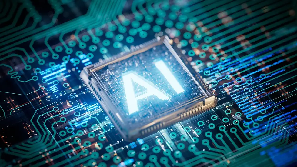
The world of computing has witnessed rapid technological advancements, particularly with the rise of artificial intelligence (AI). As AI applications become more complex, they require hardware that can keep up with ever-increasing computational demands. Traditionally, processors and chips have relied on silicon-based designs, which have reached physical limitations in terms of size and speed. However, recent breakthroughs in chip technology, such as multilayered transistor designs, photonic processors, and AI-focused hardware, have sparked new hope for the future of AI hardware. These innovations may redefine the performance, energy efficiency, and scalability of AI systems. In this article, we’ll dive into some of the most notable advancements and discuss how they pave the way for next-generation computing, transforming AI as we know it.
The Challenge of Traditional Chip Design
For decades, the semiconductor industry has relied on advances in Moore’s Law, which predicted the doubling of transistors on a chip roughly every two years. This has driven performance improvements while reducing costs. However, there’s a catch. As transistors get smaller, it becomes more difficult to maintain the performance gains promised by Moore’s Law due to heat dissipation, material limits, and quantum effects. Essentially, the physical and theoretical limits of two-dimensional (2D) chips are becoming apparent, prompting researchers to explore radical alternatives.
A key barrier has been the growing complexity of AI models and deep neural networks (DNNs) used across industries. These systems need far more computational power than conventional hardware can provide. While AI applications thrive in fields like healthcare, robotics, and data analytics, they demand specialized chips capable of handling intricate computations with minimal energy consumption. This is where the next-generation of chip designs could revolutionize AI hardware.
The Breakthrough: MIT's Multilayered Chips and Photonic Processors
Innovating with Multilayered Chips
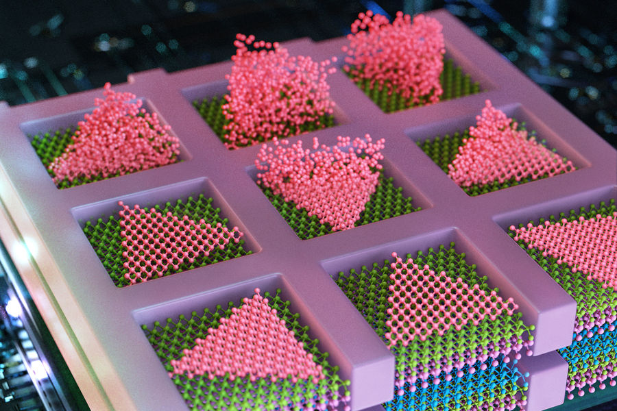
The Massachusetts Institute of Technology (MIT) has led the charge in addressing these challenges. MIT’s engineers have developed a groundbreaking technique to stack transistors vertically, which promises to create more powerful, dense, and efficient chips. By growing semiconducting materials at lower temperatures—just 380 degrees Celsius—the team bypasses the need for traditional silicon wafer substrates, which had imposed significant size and performance limitations. Their novel method could significantly accelerate computing while solving many of the size and performance limitations that have plagued traditional 2D chips.
This innovation can potentially lead to "orders-of-magnitude" improvements in computational power, especially in applications such as AI, memory, and logic processing. Dr. Jeehwan Kim, an associate professor at MIT, pointed out that this advancement could radically alter how chips are built, facilitating the development of devices that can outperform today’s supercomputers. These multilayered chips promise to process more data at faster speeds, thereby driving advancements in fields such as AI and quantum computing.
Key Advancements with Transition-Metal Dichalcogenides (TMDs)
One of the significant innovations in this new method lies in the use of transition-metal dichalcogenides (TMDs). These 2D materials, despite their atomic-scale dimensions, maintain excellent semiconducting properties. TMDs are integral for creating n-type and p-type transistors, which form the foundation of all logic operations in computing. MIT’s process allows these materials to be grown directly on top of each other, leading to faster and more efficient processing without the bulky intermediate layers found in traditional chips.
Photonic Chips: The Future of Energy-Efficient AI
Powering AI through Light
While innovations in stacking transistors represent one potential breakthrough for semiconductor design, another path to enhancing AI hardware lies in photonic chips. MIT’s Quantum Photonics and Artificial Intelligence Group, led by Dirk Englund, recently introduced a photonic processor designed to execute computations required by deep neural networks (DNNs). Photonic computing utilizes light rather than electrons to process information, and it holds promise for unprecedented speed and energy efficiency.
Current electronic chips, which use transistors to process data as electrical signals, struggle to meet the computational demands of large-scale AI models. However, light, traveling at high speeds and through specialized optical circuits, can reduce latency and energy consumption dramatically. MIT’s new photonic chip is designed to carry out both linear and nonlinear computations—vital for training DNNs—without needing to convert back and forth between optical and electronic systems.
Tackling Nonlinearities
One of the major hurdles in photonic computing is the challenge of handling nonlinear operations, a critical element for deep learning. Neurons in a neural network perform linear computations (such as matrix multiplication), but to solve complex tasks, nonlinear operations (such as activation functions) are necessary. Previously, nonlinearities were handled by electronic components, which negated some of the power advantages of photonic systems.
To solve this, the MIT team integrated nonlinear optical function units (NOFUs) within the photonic chip. These NOFUs combine both electronic and photonic elements, allowing the chip to perform the full spectrum of operations needed by a neural network, while maintaining energy efficiency and low latency. In testing, the photonic chip demonstrated 96% accuracy during training and 92% accuracy during inference, matching the performance of conventional hardware.
This breakthrough offers hope for achieving not only higher efficiency in AI hardware but also scalability for future AI applications, like self-driving cars, AI-powered diagnostics, and advanced robotics.
The Broader Implications: AI Advancements Across Industries
Both MIT’s vertical transistor stacking and photonic chip advancements signal a shift in how computational hardware is designed and utilized. As the demand for powerful AI tools grows across industries, from autonomous vehicles to AI-driven healthcare, these technological developments will serve as the foundation for the next wave of breakthroughs.
Key industries driving AI’s growth, such as healthcare, finance, and robotics, stand to benefit immensely. AI's capacity to analyze and synthesize massive volumes of data for predictive modeling, decision support, and automation will be further accelerated by hardware innovations like those discussed. For instance, AI’s role in healthcare diagnostics, disease prediction, and personalized medicine will rely on faster, more energy-efficient computing power—both of which are possible with the types of chips being developed at MIT.
As AI evolves, ensuring the availability of hardware that can keep pace with its increasing demands becomes critical. Photonic and multilayered chips may hold the key to supporting the next generation of AI capabilities.
Moving Toward Commercial Application: Scaling Up
While these developments are still in the research phase, both MIT’s photonic chips and multilayered transistor designs are poised to revolutionize AI hardware once they are scaled up. Dr. Jeehwan Kim’s spin-off company, FS2 (Future Semiconductor 2D Materials), aims to commercialize multilayered chip designs, moving the technology towards widespread use in AI chip manufacturing.
As for photonic chips, further refinements are necessary to achieve the same widespread accessibility and scalability as silicon-based chips, but the path forward is clear. Researchers aim to further reduce the reliance on electronics and increase the integration of photonics within larger systems to ensure broad application in AI data centers and edge devices.
The Future of AI Hardware
The convergence of photonics and advanced semiconductor designs promises a future of AI hardware that is more powerful, efficient, and scalable than anything we have today. The breakthroughs led by MIT and other research institutions bring us closer to realizing AI's full potential, with faster computation, lower energy consumption, and enhanced capabilities across industries.
To learn more about these cutting-edge innovations, explore how Dr. Shahid Masood and the team at 1950.ai are helping shape the AI revolution.
Comments