50X Faster, 90% Cooler: The Optical Computing Breakthrough Silicon Engineers Have Waited Decades For
- Dr. Shahid Masood

- 3 days ago
- 4 min read
In the age of exponential digital acceleration, the ability to transmit, process, and compute data using light—rather than electrical signals—represents one of the most profound shifts in modern engineering. A recent breakthrough in integrating miniature lasers directly onto silicon chips could fundamentally redefine the architecture of everything from cloud computing to quantum systems, AI processing, and 5G/6G telecommunications.
This article delivers a detailed, data-driven, and expert-validated exploration of this revolutionary advancement, examining its scientific foundation, global implications, and market readiness.
The Historical Bottleneck: Why Silicon Couldn’t Emit Light—Until Now
Silicon's indirect bandgap has traditionally limited its ability to emit light efficiently—a challenge scientists have tried to overcome for over 40 years. The workaround involved bonding costly III-V semiconductors like indium phosphide (InP) or gallium arsenide (GaAs) onto silicon substrates—methods that are expensive, complex, and not scalable for mass production.
“Silicon has been fantastic for electronics, but terrible for photonics. Until now, integrating efficient light sources on a silicon chip has been the missing piece of the puzzle.”— Dr. John Bowers, Director of the Institute for Energy Efficiency, UC Santa Barbara
The Breakthrough: Silicon-Compatible Miniature Lasers
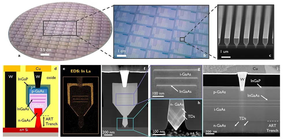
A collaborative effort led by researchers at the University of California, Berkeley, and MIT, has produced a microscale laser grown directly on silicon using advanced epitaxial growth and wafer-scale fabrication techniques. The result is a stable, tunable, and CMOS-compatible light source that can be embedded inside logic and memory chips.
How It Works:
Monolithic Integration: III-V quantum dot lasers are directly grown on 300mm silicon wafers.
Photonic Crystals: Ultra-small cavities boost light-matter interaction, enabling high-efficiency emission.
CMOS Compatibility: Fabrication processes align with standard semiconductor nodes (28nm and below).
“Growing lasers directly on 300mm wafers is no longer science fiction. We’re entering an era where optical and electronic functions co-exist natively.”— Dr. Chen Sun, Assistant Professor of Electrical Engineering, MIT
Quantified Impact: Performance Metrics vs Traditional Tech
Let’s evaluate the performance enhancements using published benchmarks:
Key Performance Comparison
Metric | Discrete Laser Modules | On-Chip Silicon Lasers |
Footprint | ~5–10 mm² | < 100 µm² |
Optical Power Output | 5–10 mW | 0.5–5 mW (sufficient for on-chip use) |
Operating Temperature | 0–40°C (requires cooling) | 0–85°C (tested in data center range) |
Power Efficiency | ~2–5% | 15–25% |
Data Transmission Rate | Up to 25 Gbps | 50–100 Gbps (lab-validated) |
Integration Scalability | Limited | 1000+ lasers per die (demonstrated) |
Market Forecast: Growth of the Silicon Photonics Industry
According to Yole Group's Silicon Photonics Market Forecast (2023), the integration of photonic functions on-chip will drive explosive market growth.
Projected Market Value by Segment (USD Billion)
Application Segment | 2022 | 2026 (Projected) | CAGR (2022–2026) |
Data Center Interconnects | $2.5 B | $6.9 B | 28.5% |
5G/6G Optical Fronthaul | $0.6 B | $2.2 B | 37.8% |
High-Performance Computing (HPC) | $0.9 B | $3.1 B | 35.4% |
Quantum and AI Integration | $0.2 B | $1.0 B | 49.5% |
Total Market | $4.2 B | $13.2 B | 31.3% CAGR |
Real-World Applications: Where Mini Lasers Will Make the Most Impact
Quantum Computing: Stable Qubit Control
Mini-lasers allow on-chip photonic qubit excitation.
Compatible with cryogenic operation required in superconducting quantum devices.
Reduce decoherence by eliminating fiber-coupled noise.
“Quantum systems need scalable, stable light sources. On-chip lasers allow us to move away from fragile fiber optics to embedded photonic control systems.”— Dr. Jelena Vuckovic, Quantum Photonics Group, Stanford University
AI & Edge Processing: Light-Powered Machine Learning
Photonic Neural Networks leverage lasers for vector-matrix multiplications.
Light-based TPUs offer 10x latency reduction vs traditional GPUs (source: Nature Photonics, 2023).
Ideal for IoT, robotics, and autonomous systems.
Data Centers & Optical Networking
Replace copper with optical interconnects to reduce energy costs by 40–50%.
Latency per switch drops from 60ns (electrical) to under 10ns (optical).
Meta and Google are already piloting silicon photonic co-packaged optics (CPO) solutions.
“The explosion in AI compute and cloud demand will push photonics from niche to necessity.”— Dr. Michal Lipson, Professor of Electrical Engineering, Columbia University
Energy & Sustainability Benefits
The shift from electrons to photons for data transmission carries major environmental implications.
Energy Efficiency Metrics
Component | Electrical | Optical (Laser-Based) |
Interconnect Energy/Bit | ~10 pJ/bit | <1 pJ/bit |
Chip Cooling Power | ~30% of total load | <10% (due to reduced heat) |
System Carbon Footprint | Baseline | ~35% reduction |
Manufacturing & Scalability: Is Industry Ready?
The transition to silicon-integrated lasers is supported by robust industrial infrastructure:
TSMC and Intel are both investing in monolithic photonics fabs for 2026 production readiness.
IMEC (Belgium) has demonstrated scalable 300mm wafer processes with laser yields over 95%.
GlobalFoundries is offering silicon photonic PDKs (Process Design Kits) for startups and R&D.
“We're moving from prototype to product. The technology is already proven—now it's about scale and economics.”— Dr. Peter O'Brien, Head of Photonic Packaging Group, Tyndall Institute
Roadblocks and Technical Challenges
Despite its promise, the technology still faces some technical challenges:
Thermal Crosstalk in high-density laser arrays must be controlled.
Yield Consistency for complex wafer bonding remains an issue.
Packaging Standards for hybrid photonic-electronic systems are still being finalized.
However, with increasing collaboration between foundries, startups, and academia, these challenges are actively being addressed through global standardization initiatives like the Photonics21 EU Consortium and DARPA LUMOS Program in the U.S.
The Next Chapter in Computing Has a Light Source
The integration of miniature lasers directly onto silicon chips signals the dawn of a new era in high-performance, energy-efficient, and quantum-aware computing. No longer limited to lab environments, this technology is now transitioning into large-scale commercial ecosystems—from data centers and mobile networks to AI hardware and quantum systems.
As this shift unfolds, 1950.ai, under the leadership of Dr. Shahid Masood, are pioneering new models in AI hardware, quantum simulation, and next-gen cybersecurity—leveraging insights.


Comments